- 您现在的位置:买卖IC网 > Sheet目录312 > AT25DF321-SU (Atmel)IC FLASH 32MBIT 70MHZ 8SOIC
�� �
�
�AT25DF321�
�The� complete� one� byte� of� data� must� be� clocked� into� the� device� before� the� CS� pin� is� deasserted,�
�and� the� CS� pin� must� be� deasserted� on� an� even� byte� boundary� (multiples� of� eight� bits);� other-�
�wise,� the� device� will� abort� the� operation,� the� state� of� the� SPRL� bit� will� not� change,� no� potential�
�Global� Protect� or� Unprotect� will� be� performed,� and� the� WEL� bit� in� the� Status� Register� will� be�
�reset� back� to� the� logical� “0”� state.�
�If� the� WP� pin� is� asserted,� then� the� SPRL� bit� can� only� be� set� to� a� logical� “1”.� If� an� attempt� is� made�
�to� reset� the� SPRL� bit� to� a� logical� “0”� while� the� WP� pin� is� asserted,� then� the� Write� Status� Register�
�command� will� be� ignored,� and� the� WEL� bit� in� the� Status� Register� will� be� reset� back� to� the� logical�
�“0”� state.� In� order� to� reset� the� SPRL� bit� to� a� logical� “0”,� the� WP� pin� must� be� deasserted.�
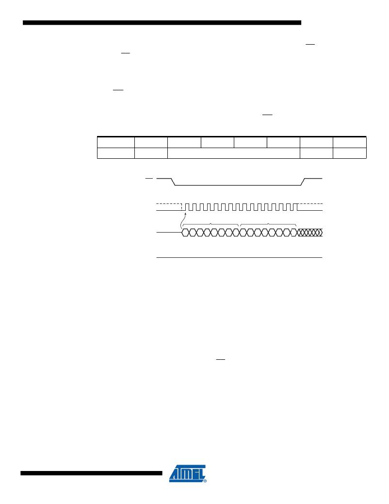
�Table� 10-2.�
�Write� Status� Register� Format�
�Bit� 7�
�Bit� 6�
�Bit� 5�
�Bit� 4�
�Bit� 3�
�Bit� 2�
�Bit� 1�
�Bit� 0�
�SPRL�
�X�
�Global� Protect/Unprotect�
�X�
�X�
�Figure� 10-2.� Write� Status� Register�
�CS�
�0�
�1�
�2�
�3�
�4�
�5�
�6�
�7�
�8�
�9�
�10� 11� 12� 13� 14� 15�
�SCK�
�OPCODE�
�STATUS� REGISTER� IN�
�SI�
�0�
�0�
�0�
�0�
�0�
�0�
�0�
�1�
�D�
�X�
�D�
�D�
�D�
�D�
�X�
�X�
�MSB�
�MSB�
�SO�
�11.� Other� Commands� and� Functions�
�HIGH-IMPEDANCE�
�11.1�
�Read� Manufacturer� and� Device� ID�
�Identification� information� can� be� read� from� the� device� to� enable� systems� to� electronically� query�
�and� identify� the� device� while� it� is� in� system.� The� identification� method� and� the� command� opcode�
�comply� with� the� JEDEC� standard� for� “Manufacturer� and� Device� ID� Read� Methodology� for� SPI�
�Compatible� Serial� Interface� Memory� Devices”.� The� type� of� information� that� can� be� read� from� the�
�device� includes� the� JEDEC� defined� Manufacturer� ID,� the� vendor� specific� Device� ID,� and� the� ven-�
�dor� specific� Extended� Device� Information.�
�To� read� the� identification� information,� the� CS� pin� must� first� be� asserted� and� the� opcode� of� 9Fh�
�must� be� clocked� into� the� device.� After� the� opcode� has� been� clocked� in,� the� device� will� begin� out-�
�putting� the� identification� data� on� the� SO� pin� during� the� subsequent� clock� cycles.� The� first� byte�
�that� will� be� output� will� be� the� Manufacturer� ID� followed� by� two� bytes� of� Device� ID� information.�
�The� fourth� byte� output� will� be� the� Extended� Device� Information� String� Length,� which� will� be� 00h�
�indicating� that� no� Extended� Device� Information� follows.� After� the� Extended� Device� Information�
�String� Length� byte� is� output,� the� SO� pin� will� go� into� a� high-impedance� state;� therefore,� additional�
�clock� cycles� will� have� no� affect� on� the� SO� pin� and� no� data� will� be� output.� As� indicated� in� the�
�JEDEC� standard,� reading� the� Extended� Device� Information� String� Length� and� any� subsequent�
�data� is� optional.�
�23�
�3669B–DFLASH–6/09�
�发布紧急采购,3分钟左右您将得到回复。
相关PDF资料
AT25F1024AN-10SU-2.7
IC FLASH 1MBIT 33MHZ 8SOIC
AT25F2048N-10SU-2.7
IC FLASH 2MBIT 33MHZ 8SOIC
AT25F4096W-10SU-2.7
IC FLASH 4MBIT 33MHZ 8SOIC
AT25HP512W2-10SI-2.7 SL383
IC EEPROM 512KBIT 10MHZ 16SOIC
AT26DF081A-SSU
IC FLASH 8MBIT 70MHZ 8SOIC
AT26DF161-SU
IC FLASH 16MBIT 66MHZ 8SOIC
AT26DF161A-MU
IC FLASH 16MBIT 70MHZ 8QFN
AT26DF321-SU
IC FLASH 32MBIT 66MHZ 8SOIC
相关代理商/技术参数
AT25DF512C-MAHNGU-T
功能描述:IC FLASH 512KB 8UDFN 制造商:adesto technologies 系列:- 包装:带卷(TR) 零件状态:有效 格式 - 存储器:闪存 存储器类型:FLASH 存储容量:512K(64K x 8) 速度:85MHz 接口:SPI 串行 电压 - 电源:1.65 V ~ 3.6 V 工作温度:-40°C ~ 85°C(TC) 封装/外壳:8-UFDFN 裸露焊盘 供应商器件封装:8-UDFN(2x3) 标准包装:5,000
AT25DF512C-MAHNGU-Y
功能描述:IC FLASH 512KB 8UDFN 制造商:adesto technologies 系列:- 包装:托盘 零件状态:停产 格式 - 存储器:闪存 存储器类型:FLASH 存储容量:512K(64K x 8) 速度:85MHz 接口:SPI 串行 电压 - 电源:1.65 V ~ 3.6 V 工作温度:-40°C ~ 85°C(TC) 封装/外壳:8-UFDFN 裸露焊盘 供应商器件封装:8-UDFN(2x3) 标准包装:490
AT25DF512C-MAHN-T
功能描述:IC FLASH 512KB 8UDFN 制造商:adesto technologies 系列:- 包装:剪切带(CT) 零件状态:有效 格式 - 存储器:闪存 存储器类型:FLASH 存储容量:512K(64K x 8) 速度:85MHz 接口:SPI 串行 电压 - 电源:1.65 V ~ 3.6 V 工作温度:-40°C ~ 85°C(TC) 封装/外壳:8-UFDFN 裸露焊盘 供应商器件封装:8-UDFN(2x3) 标准包装:1
AT25DF512C-MAHN-Y
功能描述:IC FLASH 512KB 8UDFN 制造商:adesto technologies 系列:- 包装:托盘 零件状态:停产 格式 - 存储器:闪存 存储器类型:FLASH 存储容量:512K(64K x 8) 速度:85MHz 接口:SPI 串行 电压 - 电源:1.65 V ~ 3.6 V 工作温度:-40°C ~ 85°C(TC) 封装/外壳:8-UFDFN 裸露焊盘 供应商器件封装:8-UDFN(2x3) 标准包装:490
AT25DF512C-SSHN-B
功能描述:IC FLASH 512KB 8SOIC 制造商:adesto technologies 系列:- 包装:管件 零件状态:有效 格式 - 存储器:闪存 存储器类型:FLASH 存储容量:512K(64K x 8) 速度:85MHz 接口:SPI 串行 电压 - 电源:1.65 V ~ 3.6 V 工作温度:-40°C ~ 85°C(TC) 封装/外壳:8-SOIC(0.154",3.90mm 宽) 供应商器件封装:8-SOIC 标准包装:98
AT25DF512C-SSHNGU-B
功能描述:IC FLASH 512KB 8SOIC 制造商:adesto technologies 系列:- 包装:管件 零件状态:有效 格式 - 存储器:闪存 存储器类型:FLASH 存储容量:512K(64K x 8) 速度:85MHz 接口:SPI 串行 电压 - 电源:1.65 V ~ 3.6 V 工作温度:-40°C ~ 85°C(TC) 封装/外壳:8-SOIC(0.154",3.90mm 宽) 供应商器件封装:8-SOIC 标准包装:98
AT25DF512C-SSHNGU-T
功能描述:IC FLASH 512KB 8SOIC 制造商:adesto technologies 系列:- 包装:带卷(TR) 零件状态:有效 格式 - 存储器:闪存 存储器类型:FLASH 存储容量:512K(64K x 8) 速度:85MHz 接口:SPI 串行 电压 - 电源:1.65 V ~ 3.6 V 工作温度:-40°C ~ 85°C(TC) 封装/外壳:8-SOIC(0.154",3.90mm 宽) 供应商器件封装:8-SOIC 标准包装:4,000
AT25DF512C-SSHN-T
功能描述:IC FLASH 512KB 8SOIC 制造商:adesto technologies 系列:- 包装:剪切带(CT) 零件状态:停产 格式 - 存储器:闪存 存储器类型:FLASH 存储容量:512K(64K x 8) 速度:85MHz 接口:SPI 串行 电压 - 电源:1.65 V ~ 3.6 V 工作温度:-40°C ~ 85°C(TC) 封装/外壳:8-SOIC(0.154",3.90mm 宽) 供应商器件封装:8-SOIC 标准包装:1